The first version of my open-source OpenCV–compatible FPGA Stereo Correspondence Core is now available!
(have a look at my previous FPGA Stereo Vision Project post for some more context)
It’s written purely in synthesizable Verilog, and uses device-agnostic inference for all FPGA primitives (though the current implementation is more optimized for Xilinx devices). I’m releasing it under a standard 3-clause BSD license.
The design is heavily pipelined. Under realistic conditions (in a highly-utilized, slowest-speed-grade part without any floor-planning), it can run around 150 MHz in Spartan-3E and Spartan-6 parts, and around 300 MHz in Virtex-6 parts. Much higher speeds (50+%) are possible under unrealistic (ideal) conditions.
The design is fully parameterized and highly scalable; some example implementations include:
- 320×240 @ 120 FPS in Spartan-3E 250
- 640×480 @ 30 FPS in Spartan-3E 500
- 800×480 @ 60 FPS in Spartan-6 LX25
- 800×480 @ 60 FPS in Cyclone IV EP4CE22
- 1920×1080 @ 30 FPS in Spartan-6 LX75
The core has been verified in simulation using Verilator with SystemC testbenches. Post-synthesis results (from Xilinx’s XST tool) have been verified using a simplified Verilog testbench and Xilinx’s own ISim simulator.
Scope
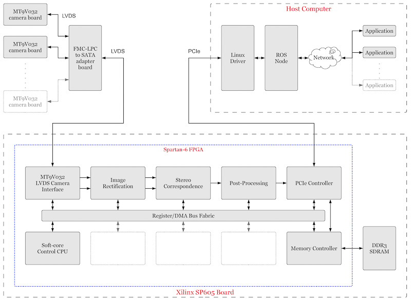
Now, before everyone runs off and tries to build their own open-source Kinect, I must stress that this isn’t a complete solution just yet; here’s a block diagram of what I have implemented:
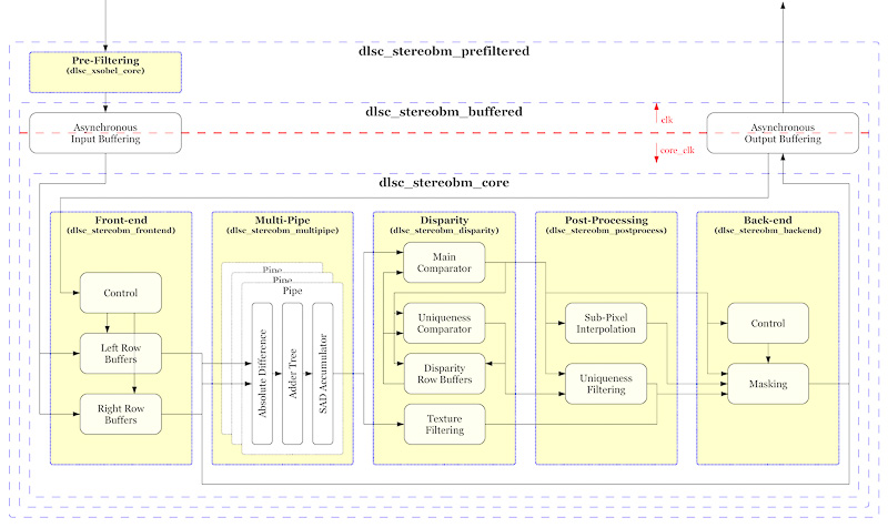
Stereo Vision Core block diagram
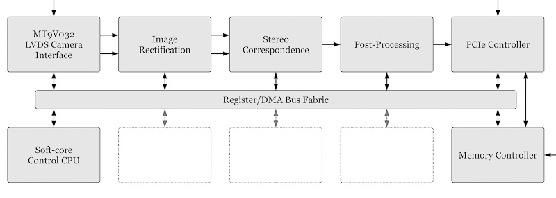
If we now refer back to the high-level block diagram that I presented before:
High-level system logic diagram
..we can see that this core implements all of the “Stereo Correspondence” block, some/all of the “Post-Processing” block and (had I actually included it on the original diagram) the “Pre-Filtering” block. While “Image Rectification” is the only significant missing image pipeline component, there’s still a lot of other system level infrastructure to develop (external interfaces, buses, etc.) before I can call the project “complete.”
That being said, the correspondence core easily represents the most critical, most resource-intensive and highest-performance component of the entire system. Completing it is a major milestone in the project.